- 您现在的位置:买卖IC网 > Sheet目录511 > SI4904DY-T1-GE3 (Vishay Siliconix)MOSFET N-CH 40V 8-SOIC
�� �
�
�Si4904DY�
�Vishay� Siliconix�
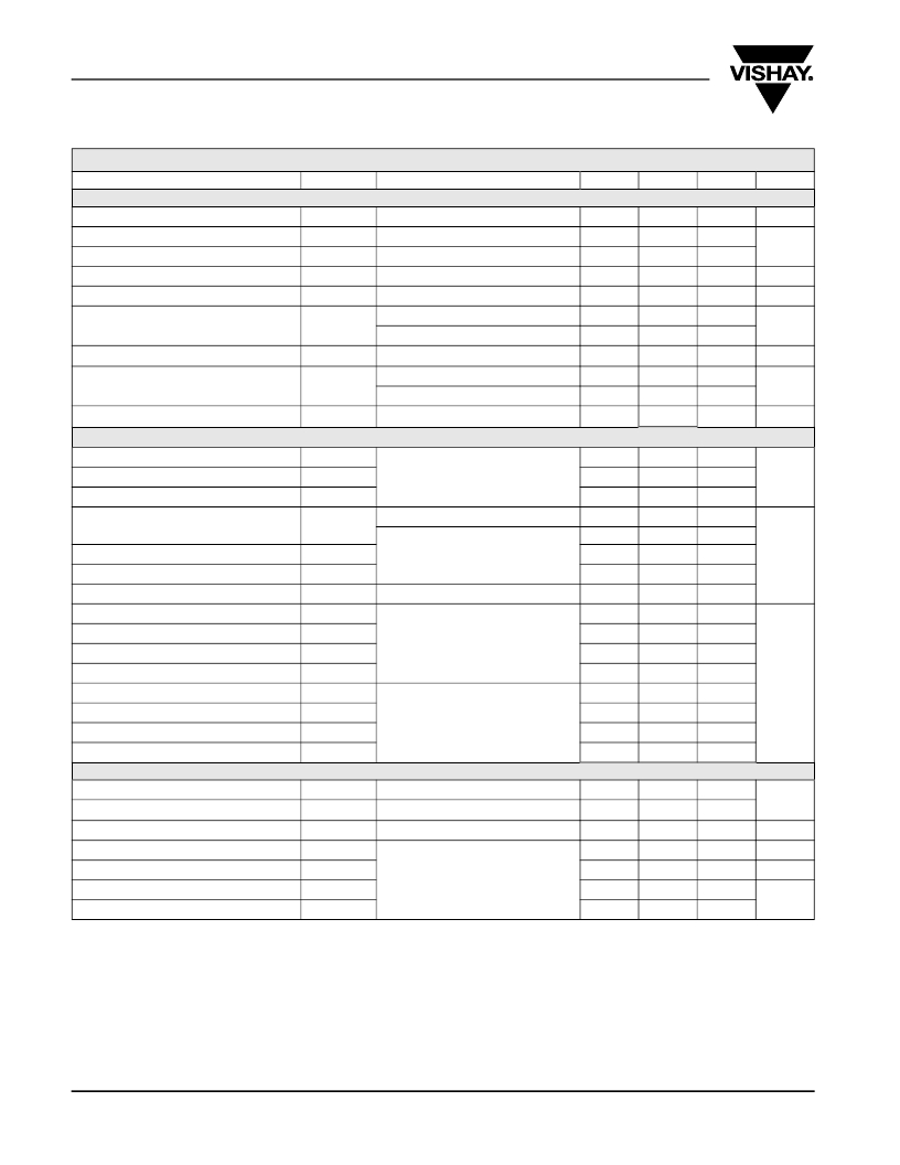
�SPECIFICATIONS� T� J� =� 25� °C,� unless� otherwise� noted�
�Parameter�
�Symbol�
�Test� Conditions�
�Min.�
�Typ.�
�Max.�
�Unit�
�Static�
�Drain-Source� Breakdown� Voltage�
�V� DS� Temperature� Coefficient�
�V� GS(th)� Temperature� Coefficient�
�V� DS�
�Δ� V� DS� /T� J�
�Δ� V� GS(th)� /T� J�
�V� GS� =� 0� V,� I� D� =� 250� μA�
�I� D� =� 250� μA�
�I� D� =� 250� μA�
�40�
�40�
�-� 4.8�
�V�
�mV/°C�
�Gate� Threshold� Voltage�
�V� GS(th)�
�V� DS� =� V� GS� ,� I� D� =� 250� μA�
�0.8�
�2.0�
�V�
�Gate-Body� Leakage�
�Zero� Gate� Voltage� Drain� Current�
�On-State� Drain� Current� b�
�I� GSS�
�I� DSS�
�I� D(on)�
�V� DS� =� 0� V,� V� GS� =� ±� 16� V�
�V� DS� =� 40� V,� V� GS� =� 0� V�
�V� DS� =� 40� V,� V� GS� =� 0� V,� T� J� =� 55� °C�
�V� DS� =� 5� V,� V� GS� =� 10� V�
�20�
�100�
�1�
�10�
�nA�
�μA�
�A�
�Drain-Source� On-State� Resistance� b�
�Forward� Transconductance� b�
�R� DS(on)�
�g� fs�
�V� GS� =� 10� V,� I� D� =� 5� A�
�V� GS� =� 4.5� V,� I� D� =� 4� A�
�V� DS� =� 15� V,� I� D� =� 5� A�
�0.013�
�0.015�
�23�
�0.016�
�0.019�
�Ω�
�S�
�Dynamic�
�a�
�Input� Capacitance�
�Output� Capacitance�
�Reverse� Transfer� Capacitance�
�Total� Gate� Charge�
�Gate-Source� Charge�
�Gate-Drain� Charge�
�Gate� Resistance�
�Turn-On� Delay� Time�
�Rise� Time�
�Turn-Off� Delay� Time�
�C� iss�
�C� oss�
�C� rss�
�Q� g�
�Q� gs�
�Q� gd�
�R� g�
�t� d(on)�
�t� r�
�t� d(off)�
�N-Channel�
�V� DS� =� 20� V,� V� GS� =� 0� V,� I� D� =� 1� MHz�
�V� DS� =� 20� V,� V� GS� =� 10� V,� I� D� =� 5� A�
�N-Channel�
�V� DS� =� 20� V,� V� GS� =� 4.5� V,� I� D� =� 5� A�
�f� =� 1� MHz�
�N-Channel�
�V� DD� =� 20� V,� R� L� =� 4� Ω�
�I� D� ?� 5� A,� V� GEN� =� 4.5� V,� R� g� =� 1� Ω�
�2390�
�270�
�165�
�56�
�26�
�5.5�
�9.7�
�2.6�
�15�
�20�
�56�
�85�
�40�
�4.0�
�23�
�30�
�85�
�pF�
�nC�
�Fall� Time�
�Turn-On� Delay� Time�
�t� f�
�t� d(on)�
�10�
�88�
�15�
�135�
�ns�
�Rise� Time�
�Turn-Off� Delay� Time�
�Fall� Time�
�t� r�
�t� d(off)�
�t� f�
�N-Channel�
�V� DD� =� 20� V,� R� L� =4� Ω�
�I� D� ?� 5� A,� V� GEN� =� 4.5� V,� R� g� =� 1� Ω�
�117�
�62�
�19�
�180�
�95�
�30�
�Drain-Source� Body� Diode� Characteristics�
�Continuous� Source-Drain� Diode� Current�
�Pulse� Diode� Forward� Current� a�
�I� S�
�I� SM�
�T� C� =� 25� °C�
�2.7�
�20�
�A�
�Body� Diode� Voltage�
�Body� Diode� Reverse� Recovery� Time�
�Body� Diode� Reverse� Recovery� Charge�
�Reverse� Recovery� Fall� Time�
�Reverse� Recovery� Rise� Time�
�V� SD�
�t� rr�
�Q� rr�
�t� a�
�t� b�
�I� S� =� 1.5� A�
�N-Channel�
�I� F� =� 2� A,� dI/dt� =� 100� A/μs,� T� J� =� 25� °C�
�0.69�
�62�
�62�
�26�
�36�
�1.2�
�95�
�95�
�V�
�ns�
�nC�
�nS�
�Stresses� beyond� those� listed� under� “Absolute� Maximum� Ratings”� may� cause� permanent� damage� to� the� device.� These� are� stress� ratings� only,� and� functional� operation�
�of� the� device� at� these� or� any� other� conditions� beyond� those� indicated� in� the� operational� sections� of� the� specifications� is� not� implied.� Exposure� to� absolute� maximum�
�rating� conditions� for� extended� periods� may� affect� device� reliability.�
�www.vishay.com�
�2�
�Document� Number:� 73793�
�S09-0540-Rev.� C,� 06-Apr-09�
�发布紧急采购,3分钟左右您将得到回复。
相关PDF资料
SI4908DY-T1-GE3
MOSFET N-CH DUAL 40V 5A 8-SOIC
SI4914BDY-T1-E3
MOSFET N-CH 30V 8-SOIC
SI4914DY-T1-E3
MOSFET DUAL N-CH 30V 8-SOIC
SI4916DY-T1-GE3
MOSFET DUAL N-CH 30V 8-SOIC
SI4920DY-T1-GE3
MOSFET DUAL N-CH 30V 8-SOIC
SI4932DY-T1-GE3
MOSFET N-CH DUAL 30V 8-SOIC
SI4933DY-T1-GE3
MOSFET P-CH DUAL 12V 8-SOIC
SI4936CDY-T1-E3
MOSFET 2N-CH 30V 5.8A SO8
相关代理商/技术参数
SI4905-C-GL
制造商:Silicon Laboratories Inc 功能描述:
SI4906DY
制造商:VISHAY 制造商全称:Vishay Siliconix 功能描述:Dual N-Channel 40-V (D-S) MOSFET
SI4906DY-T1-E3
功能描述:MOSFET DUAL N-CH 40V(D-S) RoHS:否 制造商:STMicroelectronics 晶体管极性:N-Channel 汲极/源极击穿电压:650 V 闸/源击穿电压:25 V 漏极连续电流:130 A 电阻汲极/源极 RDS(导通):0.014 Ohms 配置:Single 最大工作温度: 安装风格:Through Hole 封装 / 箱体:Max247 封装:Tube
SI4906DY-T1-GE3
功能描述:MOSFET 40V 6.6A 3.1W 39mohm @ 10V RoHS:否 制造商:STMicroelectronics 晶体管极性:N-Channel 汲极/源极击穿电压:650 V 闸/源击穿电压:25 V 漏极连续电流:130 A 电阻汲极/源极 RDS(导通):0.014 Ohms 配置:Single 最大工作温度: 安装风格:Through Hole 封装 / 箱体:Max247 封装:Tube
SI4908DY
制造商:VISHAY 制造商全称:Vishay Siliconix 功能描述:Dual N-Channel 40-V (D-S) MOSFET
SI4908DY-T1-E3
功能描述:MOSFET DUAL N-CH 40V(D-S) RoHS:否 制造商:STMicroelectronics 晶体管极性:N-Channel 汲极/源极击穿电压:650 V 闸/源击穿电压:25 V 漏极连续电流:130 A 电阻汲极/源极 RDS(导通):0.014 Ohms 配置:Single 最大工作温度: 安装风格:Through Hole 封装 / 箱体:Max247 封装:Tube
SI4908DY-T1-GE3
功能描述:MOSFET 40V 5.0A 2.75W 60mohm @ 10V RoHS:否 制造商:STMicroelectronics 晶体管极性:N-Channel 汲极/源极击穿电压:650 V 闸/源击穿电压:25 V 漏极连续电流:130 A 电阻汲极/源极 RDS(导通):0.014 Ohms 配置:Single 最大工作温度: 安装风格:Through Hole 封装 / 箱体:Max247 封装:Tube
SI4909DY
制造商:VISHAY 制造商全称:Vishay Siliconix 功能描述:Dual P-Channel 40 V (D-S) MOSFET